


Introduction
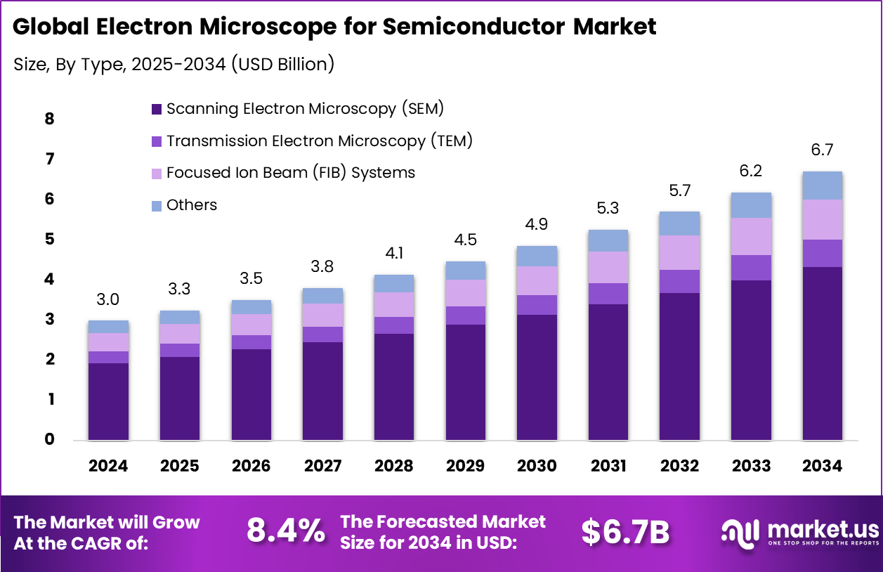
The Global Electron Microscope for Semiconductor Market is on a steady upward trajectory. In 2024, the market was valued at USD 3.0 billion, with North America commanding a 37.8 % share (USD 1.13 billion). Over the forecast period from 2025 to 2034, the market is projected to reach USD 6.7 billion, registering a CAGR of 8.4 %. This growth reflects growing demand for high-resolution imaging, defect inspection, failure analysis, and advanced process control in semiconductor manufacturing, as chip geometries shrink and complexity rises.
How Growth is Impacting the Economy
The expansion of the electron microscope market for semiconductors influences the wider economy in several ways. First, it fosters capital investment in high-end instrumentation and precision manufacturing, driving growth in sectors such as optics, vacuum systems, detectors, electronics, and software. Those upstream industries see increased demand and innovation spillovers. Second, enhanced inspection and metrology capabilities help semiconductor manufacturers reduce defects, boost yield, and accelerate node transitions – making chip production more efficient and lowering per-unit costs.
This in turn supports downstream industries (electronics, automotive, data centers, AI) by making advanced chips more accessible, enabling broader technological adoption and economic growth. Third, global competitiveness shifts: countries or regions investing in these advanced tools strengthen their semiconductor ecosystems, attract foreign direct investment, and improve their trade balance in high-tech sectors.
➤ Smarter strategy starts here! Get the sample – https://market.us/report/electron-microscope-for-semiconductor-market/free-sample/
Impact on Global Businesses
Rising Costs & Supply Chain Shifts
Adoption of electron microscopes requires substantial upfront capital, consumables (vacuum pumps, contrast agents, detectors), and skilled personnel. These equipment costs increase total capital expenditures for semiconductor firms. Moreover, supply chains shift: companies must source highly specialized components (ultra-high vacuum parts, high-resolution detectors, electron optics), often from niche suppliers. Dependency on a few critical suppliers introduces risks of supply disruptions and cost fluctuations.
Sector-Specific Impacts
- Semiconductor Fabrication: Electron microscopes are essential for defect inspection, failure analysis, overlay metrology, and new node process development.
- Memory & Storage: High density memory requires finer defect control; advanced imaging helps identify failures and optimize yield.
- Foundry & Logic Chips: As logic nodes shrink, electron microscopes become indispensable in controlling patterning and verifying structures.
- R&D / Materials: In academic and industrial research labs, electron microscopy supports material characterization for new device architectures (e.g. 3D NAND, quantum devices).
- Packaging & Heterogeneous Integration: SEM and TEM imaging for packaging defects, connections, TSVs, and interposers require sophisticated microscopes.
Strategies for Businesses
- Phase investment through pilot installations and lease-oriented capital models.
- Collaborate with instrument providers and service partnerships to share maintenance, upgrades, and training costs.
- Invest in modular add-ons (detectors, software, automation) rather than full replacement systems.
- Build in-house expertise and talent development to reduce reliance on external service providers.
- Diversify component sourcing and stock spare parts to mitigate supply chain risks.
Key Takeaways
- Strong projected growth to USD 6.7 billion by 2034 at 8.4 % CAGR
- North America holds leadership with ~37.8 % revenue share
- Growth supports semiconductor yield, innovation, and downstream industries
- Businesses face high capex, supply chain risk, and talent needs
- Strategic steps include phased deployment, partnerships, modular upgrades, and talent building
➤ Unlock growth secrets! Buy the full report – https://market.us/purchase-report/?report_id=161149
Analyst Viewpoint
At present, electron microscopy is a cornerstone technology enabling advanced semiconductor manufacturing and materials research. In the future, I foresee increasing automation, AI-aided image processing, and integration of multi-modal microscopy (e.g. combining SEM, TEM, EELS) to drive deeper insights. As throughput, ease of use, and cost per analysis improve, the technology will diffuse further into mid-tier fabs, packaging firms, and research institutions worldwide. The long-term outlook is very positive, with electron microscope tools becoming standard infrastructure in any advanced chipmaking ecosystem.
Use Cases & Growth Factors
| Use Case | Growth Factors / Drivers |
|---|---|
| Defect inspection & failure analysis | Need for high resolution detection at sub-nm scale |
| Process control & overlay metrology | Shrinking nodes require tighter tolerances |
| Materials characterization (R&D) | Novel materials, 2D materials, new architectures |
| Packaging / integration inspection | Advanced packaging, 3D stacking, TSVs, interposers |
| Throughput & automation modules | Demand for faster imaging, automated sample handling |
| Growth Drivers | Shrinking geometries, rising defect sensitivity, demand for yield improvement, R&D spending, integration with AI/image analytics, equipment automation |
Regional Analysis
North America leads with strong semiconductor infrastructure, advanced R&D and capital availability. Europe has niche strengths in materials science and specialized instrumentation. Asia Pacific is a fast-growing region, especially China, Taiwan, South Korea, Japan, and India, driven by expanding chip manufacturing and government support. These regions invest in domestic tooling and import advanced microscopes. In Latin America, the Middle East, and Africa, adoption is slower due to cost and infrastructure, but research institutions and emerging fabs present growth potential.
➤ More data, more decisions! see what’s next –
- Digital Asset Custody Market
- In-flight Internet Market
- Passive Authentication Market
- Life Insurance Market
Business Opportunities
The electron microscope market offers opportunities in component manufacturing (electron optics, detectors, vacuum systems), automation subsystems, AI analytics software, maintenance & calibration services, consumables, modular plugin modules, retrofit kits for older microscopes, training, and system integration. The growth in semiconductor fabs, R&D, packaging, and materials domains ensures a healthy demand pipeline for new systems and upgrades.
Key Segmentation
The market can be segmented by microscope type (scanning electron microscope (SEM), transmission electron microscope (TEM), scanning/transmission hybrid, focused ion beam (FIB)), application (defect analysis, process control, materials research, packaging inspection), end user (semiconductor manufacturers, research institutes, packaging firms, materials labs), and geography (North America, Europe, Asia Pacific, Rest of World). SEM typically dominates in volume, while TEM and hybrid types command higher research and advanced inspection prices.
Key Player Analysis
Competition revolves around innovation in resolution, automation, throughput, ease-of-use, and software analytics. Leading firms compete on proprietary detector technologies, multi-modal imaging capabilities, electron optics, and service networks. Differentiation comes via modular upgrade paths, AI-enabled image processing, remote diagnostics, and strong after-sales support contracts. Margins hinge on consumables, software licensure, maintenance agreements, and component supply chains.
- Thermo Fisher Scientific Company Profile
- Hitachi High-Tech India Private Limited
- Orbit & Skyline, Inc.
- JEOL Ltd.
- Nanoscience Instruments
- Leica Microsystems
- ZEISS Group
- Inquivix Technologies Inc.
- Others
Recent Developments
- Launch of a new SEM model with integrated AI-based defect classification.
- Development of cryo-TEM modules targeting failure analysis in advanced nodes.
- Introduction of automated wafer-scale imaging systems for 300 mm wafers.
- Collaborations between microscope makers and foundries to co-develop inspection standards.
- A major upgrade package was released for existing microscopes to support correlative imaging techniques.
Conclusion
The electron microscope market for semiconductors is poised for sustained growth driven by scaling demands, precision needs, and research innovation. Firms that focus on modularity, software analytics, partnerships, and talent will be best placed to capitalize on this emerging landscape.
Discuss your needs with our analyst
Please share your requirements with more details so our analyst can check if they can solve your problem(s)