Table of Contents
Introduction
FPGA Statistics: Field-programmable gate Arrays, or FPGAs, are semiconductors that provide adaptable and changeable hardware capabilities.
They contain various changeable logic units and programmable connections. Permitting individuals to craft and execute individualized digital circuits without creating their own unique silicon.
FPGAs are utilized across a range of sectors, such as telecommunications, aerospace, and industrial automation. Where there’s a need for swift creation, minimal delays, and potent computing.
Their adaptability renders them a precious asset for hardware development, research, and distinctive computing responsibilities.
Editor’s Choice
- The Global Field-Programmable Gate Array (FPGA) market is poised for steady growth in the coming years at a CAGR of 7.8%.
- In 2022, the FPGA market revenue stood at USD 6.5 billion, expected to increase to USD 13.5 billion in 2032.
- In 2022, the total low-range FPGAs contributed USD 2.3 billion. Mid-range FPGAs are at USD 1.8 billion, and high-range FPGAs generate USD 2.4 billion.
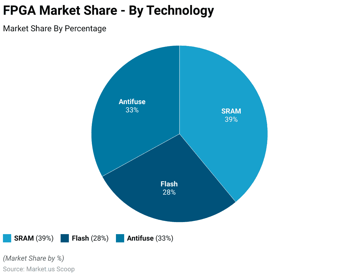
- As of the latest data, SRAM-based FPGAs dominate the market with a 39% share.
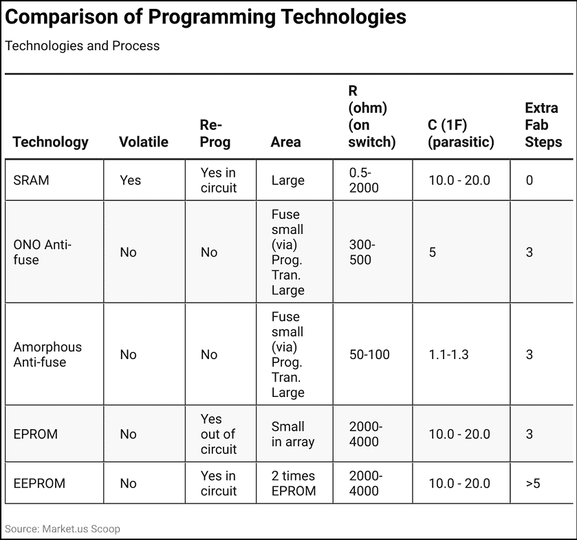
- Resistance (R) on the switch and parasitic capacitance (C) play essential roles in signal propagation. With ONO anti-fuse FPGAs have moderate resistance (300-500 ohms) and low capacitance (5F). While amorphous anti-fuse FPGAs exhibit lower resistance (50-100 ohms) and slightly higher capacitance (1.1-1.3F).
- The Cyclone V consists of two primary elements: the FPGA segment and a hard processor system (HPS) centered around a single- or dual-core 32-bit Arm Cortex-A9 MPCORE clocked at 925 MHz.
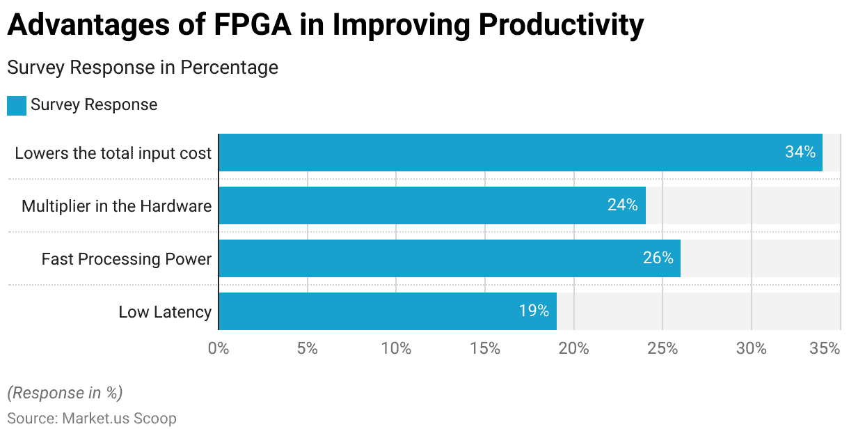
- 34% of respondents appreciate FPGAs’ capability to lower the total input cost, making them a cost-effective solution in various applications.
Global FPGA Market Statistics
FPGA Market Size Statistics
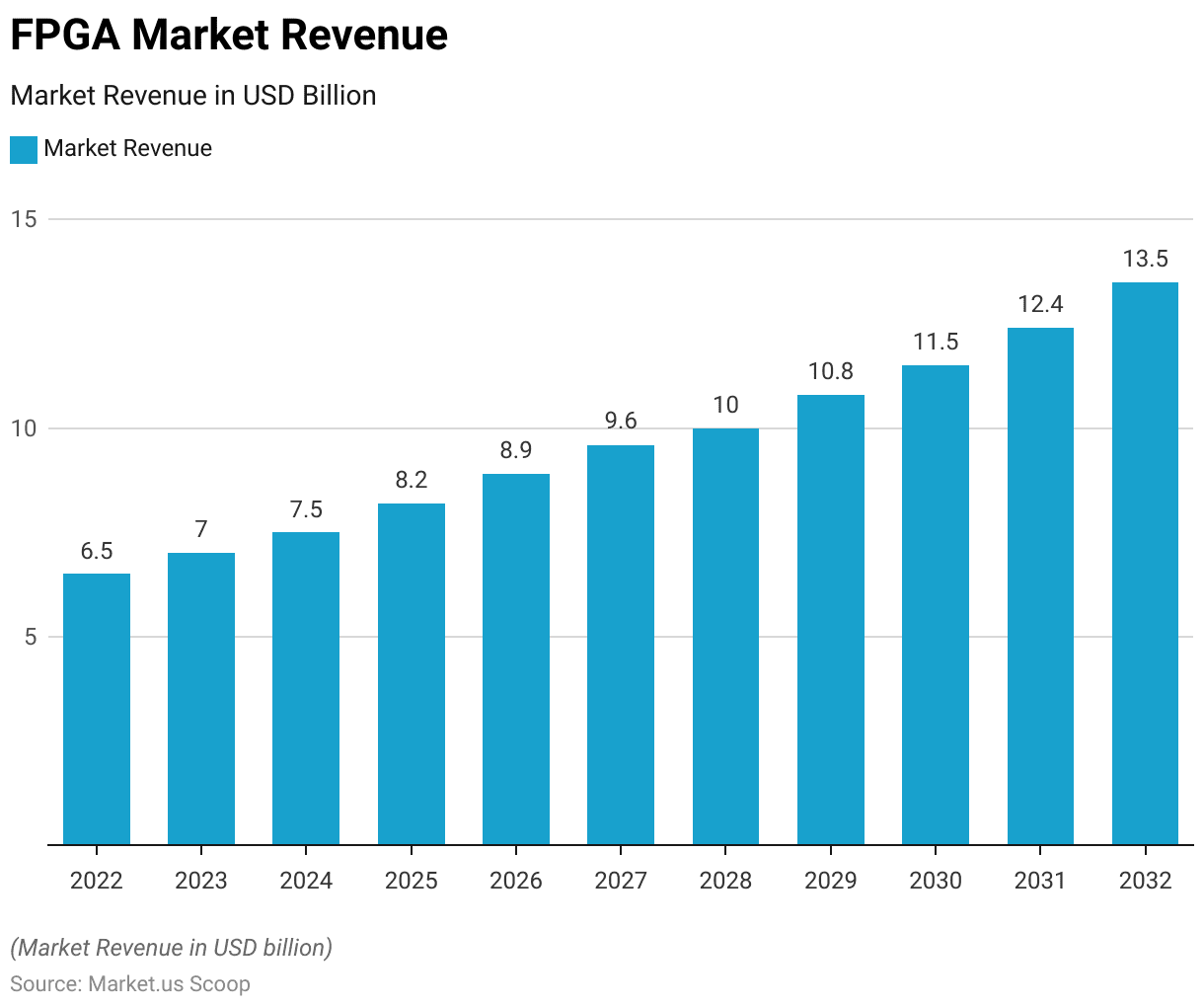
- The Global Field-Programmable Gate Array (FPGA) market is poised for steady growth in the coming years at a CAGR of 7.8%.
- In 2022, the FPGA market revenue stood at USD 6.5 billion, expected to increase to USD 7.0 billion in 2023.
- The growth continues with revenues of USD 7.5 billion in 2024, USD 8.2 billion in 2025, and USD 8.9 billion in 2026.
- As we move further, the market is forecasted to reach USD 9.6 billion in 2027, USD 10.0 billion in 2028, and USD 10.8 billion in 2029.
- The trend of growth is set to persist, with revenues projected to reach USD 11.5 billion in 2030, USD 12.4 billion in 2031, and USD 13.5 billion in 2032.
- This upward trajectory underscores FPGA technology’s increasing importance and adoption across various industries, driving its market expansion in the years to come.
(Source: market.us)
FPGA Market Size – by Configuration Statistics
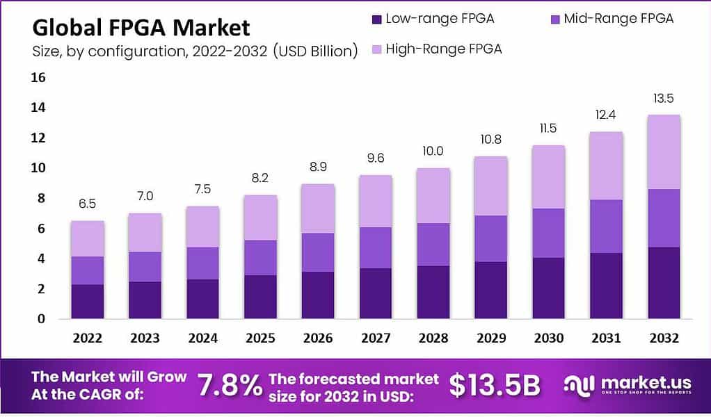
- The Global Field Programming Gate Array (FPGA) market is projected to experience steady growth over the next decade.
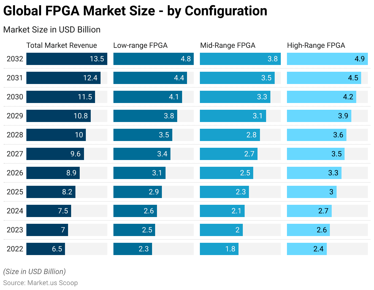
- In 2022, the total market revenue stood at USD 6.5 billion, with low-range FPGAs contributing USD 2.3 billion, mid-range FPGAs at USD 1.8 billion, and high-range FPGAs generating USD 2.4 billion.
- As we move into 2032, the market is expected to expand significantly, reaching a total revenue of USD 13.5 billion.
- This growth will be driven by the increasing demand for FPGAs across various industries.
- Low-range FPGAs are anticipated to reach USD 4.8 billion, mid-range FPGAs at USD 3.8 billion, and high-range FPGAs makeup USD 4.9 billion of the total market revenue.
- This upward trajectory reflects the vital role that FPGAs play in enabling customizable and adaptable hardware solutions for a wide range of applications, from telecommunications to automotive and beyond.
(Source: market.us)
Field Programming Gate Array Market Share – by Technology Statistics
- Technology’s market share distribution reveals an intriguing landscape in the global Field Programming Gate Array (FPGA) market.
- As of the latest data, SRAM-based FPGAs dominate the market with a 39% share. These FPGAs are known for their reconfigurability and speed. Are favored in applications where flexibility and quick turnaround times are crucial.
- Following closely behind are Flash-based FPGAs, capturing a substantial 28% market share. Flash FPGAs are valued for their non-volatile configuration storage. Making them ideal for applications requiring data persistence and security.
- Lastly, Antifuse-based FPGAs hold a notable 33% market share. Antifuse technology is preferred when reliability and security are paramount. As it offers a one-time programmable configuration that cannot be altered once set.
- This technology diversity within the FPGA market underscores the importance of tailoring hardware solutions to specific application requirements. Ensuring that many industries benefit from these versatile devices.
(Source: market.us)
Comparison Statistics of Different FPGA Programming Technologies
- When comparing different FPGA programming technologies, several key factors come into play.
- First, we consider volatility, with SRAM-based FPGAs allowing for volatile reprogramming in-circuit. In contrast, anti-fuse-based FPGAs, both ONO and amorphous types, offer non-volatile programming. Making them suitable for applications where data persistence is critical.
- Next, regarding the area and electrical characteristics, SRAM-based FPGAs tend to have larger area footprints than the anti-fuse variants. Which feature small fuse elements and programming transistors.
- Resistance (R) on the switch and parasitic capacitance (C) play essential roles in signal propagation, with ONO anti-fuse FPGAs having moderate resistance (300-500 ohms) and low capacitance (5F), while amorphous anti-fuse FPGAs exhibit lower resistance (50-100 ohms) and slightly higher capacitance (1.1-1.3F).
- Additionally, the extra fabrication steps required for each technology vary. SRAM FPGAs typically involve no extra fabrication steps, making them relatively straightforward.
- In contrast, both ONO and amorphous anti-fuse FPGAs require additional steps for fuse creation and programming transistors.
- Furthermore, while offering non-volatile reprogramming, EPROM and EEPROM-based FPGAs involve extra fabrication steps and slightly larger area footprints than anti-fuse options.
- When choosing the most suitable FPGA programming technology for a particular application. These considerations highlight the trade-offs between volatility, programmability, area, and electrical characteristics.
(Source: Department of Electrical and Computer Engineering, University of Toronto)
FPGA Architecture Statistics
- Fundamentally, an FPGA’s architecture consists of many vital elements called configurable logic blocks (CLBs). These CLBs are encircled by a system of adaptable connections, commonly called a fabric, which facilitates the routing of signals between these CLBs.
- Moreover, input/output (I/O) blocks connect the FPGA to external devices. Depending on the particular manufacturer, these CLBs might be denoted by alternate terms like logic blocks (LBs), logic elements (LEs), or logic cells (LCs).
- Within an individual CLB, you’ll find multiple logic blocks. An important component of an FPGA is the lookup table (LUT), which is a defining feature. LUTs store a predetermined set of logical results for every possible input combination.
- Typically, LUTs with four to six input bits are extensively employed. Standard logic functions like multiplexers (mux), full adders (FAs), and flip-flops are frequently encountered within this context.
- The configuration and layout of components within the CLB can vary between devices. Typically, it includes two three-input LUTs, a full adder, a D-type flip-flop, and a standard multiplexer.
- Additionally, there are two extra multiplexers, which are set up during FPGA programming.
- This simplified CLB serves a dual purpose. In its standard mode, the LUTs combine with Mux 2 to create a four-input LUT. In contrast, in arithmetic mode, the LUT outputs become inputs for the full adder, along with a carry input from another CLB.
- Mux 4 selects either the full adder’s output or the LUT output. Mux 6 determines if the operation is asynchronous or synchronized with the FPGA clock through the D flip-flop.
- In the latest FPGA generations, CLBs have become more complex, capable of handling multiple tasks within a single block. They can combine to perform advanced functions like multiplication, data storage, counting, and even digital signal processing (DSP) tasks.
(Source: Arrow)
SoC FPGA Statistics
- SoC FPGAs, short for System-on-Chip Field-Programmable Gate Arrays, offer various processing capabilities tailored to diverse applications.
- Take, for example, Intel’s Cyclone V, a cost-effective and energy-efficient SoC FPGA.
- It’s designed to excel in high-volume scenarios, such as controlling industrial motors, bridging protocols, handling video processing tasks, and powering portable devices.
- The Cyclone V consists of two primary elements: the FPGA segment and a hard processor system (HPS) centered around a single- or dual-core 32-bit Arm Cortex-A9 MPCORE clocked at 925 MHz.
- Both segments come equipped with their collection of peripheral components, which may include specialized hardware from third-party suppliers.
- In sharp contrast, the Stratix 10 SX targets high-performance applications like communication systems, accelerating data centers, powering high-performance computing (HPC) setups, processing radar data, and serving as a platform for ASIC prototyping.
- This FPGA shines with its quad-core 64-bit Arm Cortex-A53 processors capable of running at speeds of up to 1.5 GHz.
(Source: Arrow)
Key FPGA Components Statistics
Configurable Logic Blocks
- The core element of a field programmable gate array (FPGA) is the Configurable Logic Block (CLB). This is a logic cell that can be configured to perform specific functions.
- These CLBs are connected through a connection block, which includes essential components like carry and control logic, transistor pairs, and lookup tables (LUTs) to handle the required logical operations in a design.
- To create a CLB, you can use logic-based multiplexers or LUTs. In LUT-based logic, a CLB consists of a D flip-flop, a lookup table, and a 2:1 multiplexer.
- Flip-flops serve as storage elements while the multiplexer selects the appropriate output.
- CLBs are further organized into columns and pairs, each containing a specific number of slices.
(Source: Spice Works)
Programmable Interconnects
- In FPGAs, this region handles the distinctive connections among logic cells in various blocks. Switch boxes containing multiple semiconductor switches are commonly used for this purpose.
- These electrically programmable links serve as the routes for transmitting signals between logic blocks.
- The routes consist of wire segments of different lengths, interconnected by electrically programmable switches.
- The number of components allotted for these pathways influences the FPGA’s density.
- These programmable links are essential as they connect outputs from one section or input pad of the FPGA to any other cell or pad in the circuit.
(Source: Spice Works)
Programmable Routing
- Programmable routing is critical, often occupying more than half of the fabric surface and affecting application latency.
- It comprises pre-made wire segments and pre-set switches.
- Configuring the right switch combination, any output from a function block can be connected to any input. There are two fundamental routing architectures in field-programmable gate arrays (FPGAs).
- Designs follow a hierarchy, with higher-level components incorporating lower-level modules and connecting signals. This approach drives the need for hierarchical FPGAs.
- Further, these hierarchical FPGAs can establish connections using short wires that link discrete parts of a chip, as communication typically occurs between closely related modules in the design hierarchy.
- The routing design influences the density and performance of the FPGA.
(Source: Spice Works)
Programmable I/O Blocks
- Interfacing pins are vital for connecting logic blocks to external components in an FPGA. This connection point between the FPGA and external circuits is called the Input Output Block (IOB).
- IOBs are programmable input and output devices tailored to handle the diverse requirements of input/output signals with varying electrical characteristics.
- These IO blocks are the crucial link bridging the routing architecture and configurable logic blocks (CLBs) with external elements.
- These IO blocks establish one-way or two-way programmable links, connecting the package pins to the device’s internal circuitry.
- Unlike earlier FPGAs without built-in processors, modern FPGAs offer versatility for various applications.
- Further, this means an FPGA can be programmed for simple functions like an OR gate or more complex tasks, even as a multi-core processor, depending on the specific application needs.
(Source: Spice Works)
On-chip Memory
- Initially, FFS (Flip-Flops) integrated within the FPGA’s logic blocks served as the initial form of on-chip memory.
- However, as the logic capacity of field-programmable gate arrays (FPGAs) improved, they began to be used in larger systems, which consistently required on-chip memory to store and reuse data efficiently.
- Building extensive RAMs from registers and LUTs proved significantly less space-efficient, about 100 times less dense than an SRAM block. As a result, the need for denser on-chip storage became evident.
- Furthermore, the memory requirements of applications running on FPGAs can vary greatly.
(Source: Spice Works)
Advantages of FPGA Statistics
- As survey responses indicate, FPGAs offer several advantages that significantly enhance productivity.
- A notable advantage is their ability to provide low latency, cited by 19% of respondents. This means that FPGAs can rapidly process data, reducing delays in various applications.
- Another key benefit highlighted by 26% of respondents is their fast processing power, enabling swift execution of complex tasks.
- FPGAs also excel in handling multiplication operations directly in hardware, a feature valued by 24% of those surveyed.
- Additionally, 34% of respondents appreciate FPGAs’ capability to lower the total input cost, making them a cost-effective solution in various applications.
- These advantages collectively position FPGAs as a valuable tool for improving productivity across various industries and use cases.
(Source: Embedded Computer Design)
FPGA Cost Statistics
- Brand-new FPGAs typically come with a price tag exceeding $10,000, whereas new GPUs are generally priced at several hundred to several thousand dollars.
- It’s worth noting that FPGA prices tend to decrease over time, and smaller and more affordable FPGA options are available.
- However, if a designer aims to utilize the latest and largest FPGA, they should anticipate a cost of at least $10,000 for the FPGA device alone.
- Moreover, what makes matters more challenging is that this price doesn’t cover additional expenses such as those incurred for board vendors, IP vendors, and necessary tools, all of which can significantly contribute to the overall cost.
(Source: University of Florida)
Recent Developments
Acquisitions and Mergers:
- AMD acquires Xilinx: In 2023, AMD completed its acquisition of Xilinx, a leading player in the field-programmable gate array (FPGA) market, in a deal valued at $35 billion. This acquisition strengthens AMD’s position in high-performance computing and data center markets, integrating Xilinx’s FPGA expertise to offer more flexible, adaptive computing solutions.
- Intel acquires eASIC: Intel expanded its FPGA portfolio by acquiring eASIC, a structured ASIC company, for $300 million in early 2023. This acquisition aims to provide Intel with a broader range of customizable hardware solutions for data centers, 5G, and IoT applications.
New Product Launches:
- Xilinx Versal ACAP: In 2023, Xilinx (now part of AMD) launched the Versal ACAP (Adaptive Compute Acceleration Platform), which integrates FPGA with adaptive processing capabilities. This new product offers high-performance computing, AI acceleration, and flexible hardware reconfiguration, targeting data centers and telecommunications.
- Intel Agilex 7 FPGAs: Intel introduced the Agilex 7 FPGA series in 2024, designed for advanced workloads in data centers, 5G networks, and AI inference. These FPGAs offer improved power efficiency, enhanced compute density, and better support for next-gen applications.
Funding:
- Flex Logix secures $60 million in funding: Flex Logix, an emerging player in the FPGA space, raised $60 million in 2023 to accelerate the development of its eFPGA (embedded FPGA) technology. This funding will help Flex Logix enhance its R&D capabilities and expand its market presence in AI and edge computing.
- Achronix raises $100 million for AI-driven FPGA development: Achronix, a provider of high-performance FPGA solutions, secured $100 million in early 2024 to focus on AI and machine learning applications. The company aims to create FPGAs optimized for AI inference workloads, targeting edge computing and data center markets.
Technological Advancements:
- AI and Machine Learning Integration: AI-driven FPGAs are gaining traction due to their flexibility and ability to accelerate machine learning workloads. By 2024, it is projected that over 40% of data centers will adopt AI-driven FPGAs, significantly improving processing efficiency for complex AI tasks.
- eFPGA for Custom Solutions: Embedded FPGAs (eFPGA) are being increasingly used in custom chip designs for specific applications, offering flexibility and lower development costs. eFPGAs are particularly popular in 5G and IoT, where adaptability is crucial for emerging technologies.
Market Dynamics:
- Growth in the FPGA Market: This growth is driven by the increasing demand for reprogrammable hardware in sectors like automotive, telecommunications, and data centers.
- Rising Demand in AI and 5G: AI and 5G are major growth drivers for the FPGA market, with FPGAs providing the flexibility and performance required for these cutting-edge technologies. By 2025, AI and 5G applications are expected to account for over 30% of FPGA deployments, especially in data processing and communication systems.
Conclusion
FPGA Statistics – Field-Programmable Gate Arrays (FPGAs) are versatile semiconductor devices used in industries like telecommunications, aerospace, and industrial automation for their flexibility and reconfigurability.
They consist of configurable logic blocks (CLBs) and programmable interconnects, allowing custom digital circuit designs without custom silicon.
SoC FPGAs merge FPGA fabric with embedded processors for various applications. While FPGAs offer low latency, fast processing, and cost advantages, they are more expensive than GPUs, especially for larger models.
Additional expenses from board vendors, IP vendors, and tools can contribute significantly to the overall cost.
FAQs
An FPGA, or Field-Programmable Gate Array, is a semiconductor device that allows users to design and implement custom digital circuits. Unlike traditional fixed-function chips, FPGAs are reconfigurable, offering flexibility in hardware design.
FPGAs consist of configurable logic blocks (CLBs) and programmable interconnects. Users program the CLBs to perform specific functions, and the interconnects route signals between these blocks, allowing for custom circuit designs.
FPGAs are used in various industries, including telecommunications, aerospace, industrial automation, and more. They are valuable for rapid prototyping, low-latency processing, and high-performance computing tasks.
FPGAs are reprogrammable, making them flexible for iterative design changes, while ASICs are custom-designed for specific functions and are not reprogrammable.
FPGAs offer low latency, fast processing power, and the ability to handle custom logic functions. They can reduce total input costs for certain applications.
Discuss your needs with our analyst
Please share your requirements with more details so our analyst can check if they can solve your problem(s)


