


Table of Contents
Introdcuction
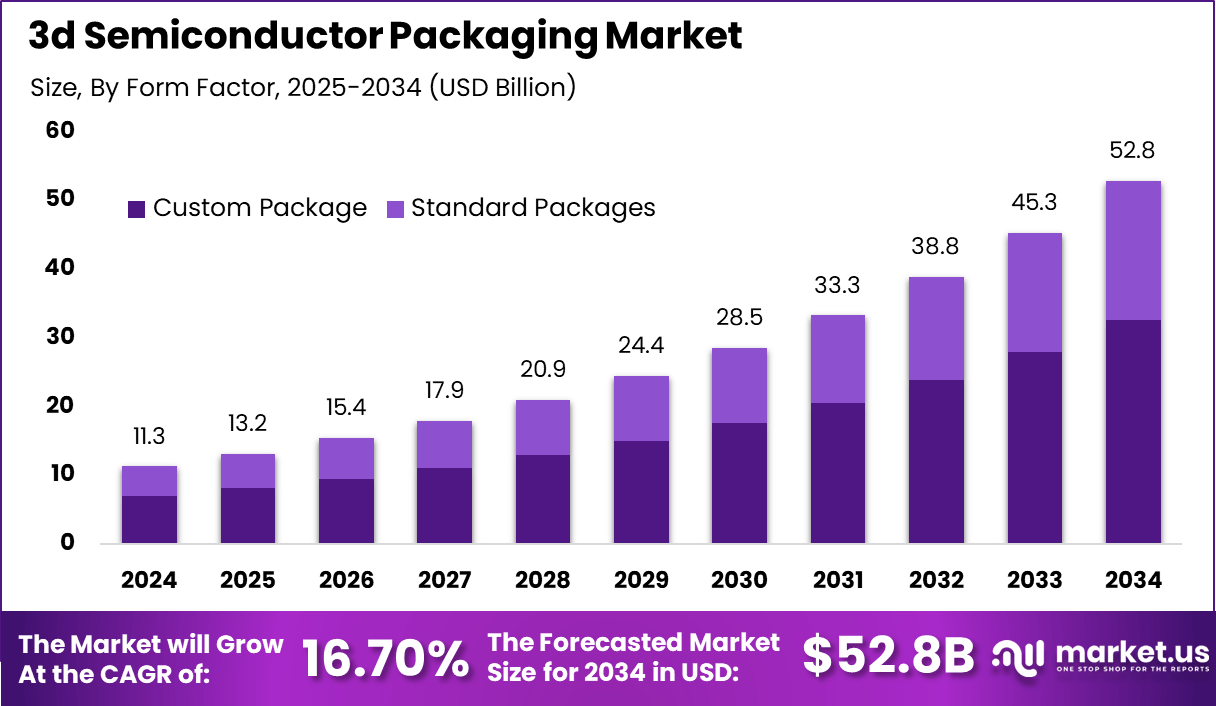
The Global 3d Semiconductor Packaging Market generated USD 11.3 billion in 2024 and is predicted to register growth from USD 13.2 billion in 2025 to about USD 52.8 billion by 2034, recording a CAGR of 16.70% throughout the forecast span. In 2024, Asia Pacific held a dominant market position, capturing more than a 41.2% share, holding USD 4.64 Billion revenue.
3D semiconductor packaging is an advanced approach that stacks multiple semiconductor components vertically to improve performance, reduce space, and enhance functionality. Instead of placing chips side by side, this method connects them in layers, allowing faster data transfer and better integration within a compact design.
It is widely used in high performance computing, memory devices, and consumer electronics where speed and efficiency are critical. As electronic devices become smaller and more powerful, 3D packaging is playing an important role in supporting next generation chip designs.
One of the main driving factors is the growing demand for higher performance and energy efficient electronic systems. Traditional packaging methods are reaching physical and technical limits, which is pushing the industry toward more advanced solutions.
In addition, the rise of applications such as artificial intelligence, data centers, and mobile computing is increasing the need for faster data processing and improved bandwidth. 3D packaging helps meet these requirements by reducing signal delay and improving communication between components. The focus on miniaturization in electronics is also encouraging the use of stacked designs that can deliver more functionality within limited space.
Demand for 3D semiconductor packaging is increasing as manufacturers look for ways to enhance chip performance while maintaining compact form factors. There is a strong preference for solutions that can support complex designs and provide reliable connections between layers.
Companies are also seeking technologies that can improve thermal management and ensure stable operation under high workloads. The demand is particularly strong in sectors that require high speed processing and efficient power usage. As electronic devices continue to evolve and become more advanced, the need for innovative packaging solutions is expected to grow steadily.
Top Key Market Segment
- Through-silicon via technology commands 35.8%, enabling vertical interconnects for high-density stacking, reduced form factors, and improved signal integrity in multi-die integration.
- Consumer electronics application captures 40.3%, powering smartphones, wearables, and AR/VR devices with heterogeneous integration for enhanced performance and battery efficiency.
- Organic substrates hold 52.4% by material type, providing cost-effective thermal management, fine-pitch routing, and compatibility with fan-out wafer-level packaging.
- Electronics manufacturers lead end-users at 64.9%, leveraging 3D packaging for supply chain localization, yield optimization, and rapid prototyping cycles.
- Custom packages dominate form factor at 61.6%, supporting application-specific SiP designs with embedded passives and integrated antennas.
- Back-end processing claims 76.1%, focusing on wafer thinning, bonding, and final test to enable heterogeneous integration at scale.
- Asia-Pacific drives 41.2% global value, with China at USD 1.41 billion and 12.2% CAGR, fueled by smartphone OEMs, memory stacking advances, and government semiconductor initiatives.
How AI is Reshaping the Future of this market?
Artificial intelligence is becoming a core force behind the evolution of the 3D semiconductor packaging market, influencing both demand and technological innovation across the value chain. AI workloads are significantly increasing the need for advanced chip architectures. Applications such as machine learning and data analytics require high processing power and faster data transfer between components. This is accelerating the shift toward 3D stacking and chiplet-based designs, where multiple layers of chips are integrated vertically. These structures reduce latency and improve bandwidth, making them highly suitable for AI-driven systems.
AI is also transforming how semiconductor packages are designed. Advanced algorithms are now used to simulate complex 3D structures, optimize interconnect layouts, and predict thermal behavior. This reduces reliance on manual design processes and allows faster development cycles. As packaging complexity increases, AI-driven tools help engineers achieve better accuracy and performance in a shorter time.
Another major shift is the adoption of system-level co-design. AI enables simultaneous optimization of chip design, packaging, and system performance. Instead of treating each layer separately, AI models evaluate multiple parameters such as power consumption, heat dissipation, and signal integrity together. This approach is critical in 3D packaging, where small design changes can impact overall system efficiency.
In manufacturing, AI is improving process control and yield rates. It is widely used for defect detection, quality inspection, and predictive maintenance. AI-powered systems can identify microscopic defects in stacked chips and ensure consistency in complex processes. This helps reduce production losses and improves overall efficiency.
Thermal management is another area where AI is playing a key role. 3D packaging increases power density, leading to higher heat generation. AI models are used to simulate thermal performance and optimize cooling solutions. This enhances reliability and ensures stable performance in high-demand AI applications.
AI is also accelerating innovation in packaging technologies and materials. It is driving the development of advanced solutions such as hybrid bonding, high-density interconnects, and new substrate materials that support faster and more efficient data transfer.
Overall, AI is reshaping the 3D semiconductor packaging market by increasing demand for high-performance solutions while also improving design, manufacturing, and reliability processes. It is turning semiconductor packaging into a critical enabler of next-generation computing systems.
Driver
The 3D semiconductor packaging market is driven by the rising demand for compact and high-performance electronic systems. As devices become smaller and more powerful, manufacturers are shifting toward vertical chip stacking to improve speed and reduce signal delay. This approach allows multiple components to be integrated into a single package, enhancing efficiency and performance across modern applications.
Another factor supporting this driver is the increasing use of advanced technologies such as artificial intelligence, connected devices, and high-performance computing. These applications require faster data transfer and higher bandwidth, which traditional packaging struggles to deliver. 3D packaging helps meet these needs by enabling tighter integration and improved communication between chips.
Restraint
A key restraint in the market is the high complexity involved in manufacturing 3D semiconductor packages. The process requires advanced techniques such as precise alignment and multi-layer integration, which demand specialized equipment and expertise. This complexity can slow production and make it difficult for manufacturers to scale operations efficiently.
Another limiting factor is the challenge of heat management within stacked chip structures. As multiple layers generate heat in a confined space, it becomes difficult to maintain stable operating conditions. Poor thermal control can impact performance and reliability, which discourages wider adoption in certain applications.
Opportunity
A major opportunity in the market lies in the growing demand for advanced computing systems across industries. Sectors such as automotive, healthcare, and telecommunications are adopting more intelligent and connected solutions, creating a need for powerful yet compact semiconductor designs. 3D packaging supports this shift by enabling higher functionality within limited space.
Another opportunity is the development of heterogeneous integration, where different types of chips are combined into a single package. This approach allows greater flexibility in design and supports the creation of multifunctional systems. It opens new possibilities for innovation in emerging technologies and expands the application scope of advanced packaging solutions.
Challenge
One of the main challenges in the market is the shortage of skilled professionals required to design and manufacture complex 3D structures. The process involves advanced knowledge in areas such as system integration and thermal management. A limited talent pool can slow development and restrict the pace of innovation.
Another challenge is maintaining consistent quality and reliability during production. As chip designs become more complex, even minor defects can affect overall performance. Ensuring proper testing and alignment across multiple layers adds to the difficulty, making quality control a critical concern for manufacturers.
Key Market Segment
By Technology
- Through-Silicon Via (TSV)
- Micro-Bump Technology
- Wafer-Level Packaging (WLP)
- Fan-Out Packaging
By Application
- Consumer Electronics
- Automotive
- Telecommunications
- Industrial
By Material Type
- Silicon
- Organic Substrates
- Ceramics
By End-User
- Electronics Manufacturers
- Automotive Manufacturers
- Telecommunications Providers
- Industrial Equipment Manufacturers
By Form Factor
- Standard Packages
- Custom Package
By Processing Type
- Front-End Processing
- Back-End Processing
Competetive Analysis
The competitive landscape of the 3D Semiconductor Packaging Market is dominated by large semiconductor manufacturers and packaging specialists with strong technological capabilities. Companies such as TSMC (Taiwan Semiconductor Manufacturing Company), Intel Corporation, Samsung Electronics, ASE Group (Advanced Semiconductor Engineering), Amkor Technology, and Siliconware Precision Industries Co., Ltd. (SPIL) focus on advanced packaging technologies including 3D stacking, system-in-package, and chiplet integration.
These players invest heavily in research and development to improve performance, reduce power consumption, and support high-density integration for applications like AI, high-performance computing, and mobile devices. Their strong manufacturing capabilities and global presence help them maintain a leading position in the market.
At the same time, companies such as Broadcom Inc., Micron Technology, Qualcomm Incorporated, NXP Semiconductors, ON Semiconductor, STMicroelectronics, Texas Instruments, Renesas Electronics Corporation, and Infineon Technologies focus on integrating advanced packaging into their semiconductor products to enhance functionality and efficiency.
Players like GlobalFoundries, Marvell Technology Group, Sony Corporation, Lattice Semiconductor Corporation, and Jiangsu Changjiang Electronics Technology Co. also compete by offering specialized solutions and expanding their packaging capabilities. Competition in this market is driven by innovation in chip integration, demand for smaller and faster devices, and the ability to deliver cost-effective and scalable packaging solutions.
Recent Development
- January, 2026 – Broadcom Jericho3-AI uses 3D CoPoSi stacking linking 128x 200G SerDes for 6.4Tbps switches. Organic interposer handles PAM4 signaling while LPDDR6X caches boost lookup 60%. Networking silicon leader.
- March, 2026 – Infineon CoolSiC Gen3 3D modules vertically stack 12 MOSFET dies cutting EV traction inverter volume 45%. Ag sintering replaces solder while split-gate SiC boosts switching 3x faster. Power semiconductor pioneer.
Conclusion
The 3D semiconductor packaging market is expected to show steady growth as demand for high performance and compact electronic devices continues to rise. This growth is driven by increasing use of advanced chips in areas such as artificial intelligence, data centers, and consumer electronics, where speed, power efficiency, and space saving are important. Companies are focusing on improving chip integration and performance through advanced packaging methods, which is helping the market expand further.
At the same time, the market faces some challenges related to high manufacturing complexity and cost, along with technical issues in heat management and design. However, ongoing innovation and investment in research are helping to address these concerns. As industries continue to move toward smaller and more powerful devices, the adoption of 3D semiconductor packaging is expected to increase, making it an important part of the future semiconductor ecosystem.
Discuss your needs with our analyst
Please share your requirements with more details so our analyst can check if they can solve your problem(s)