


Table of Contents
Report Overview
A semiconductor photomask is a crucial component in the microfabrication of integrated circuits and patterned films for semiconductor devices. It is essentially a template that transfers a circuit’s design onto a semiconductor wafer, influencing the precise geometries of microchips. This process is integral to the semiconductor manufacturing industry, as it defines the paths for electrical currents in various types of electronic devices.
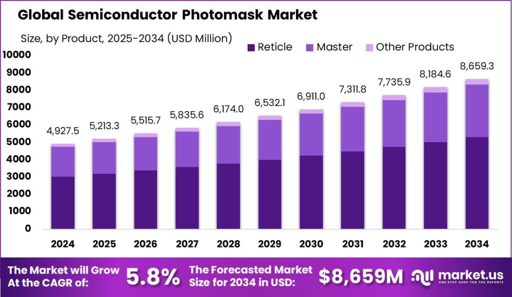
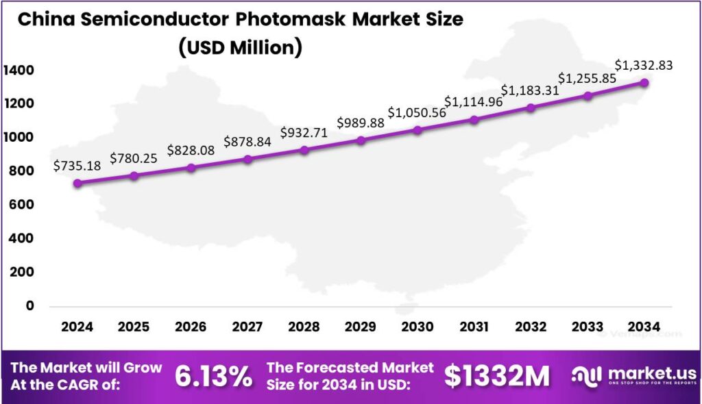
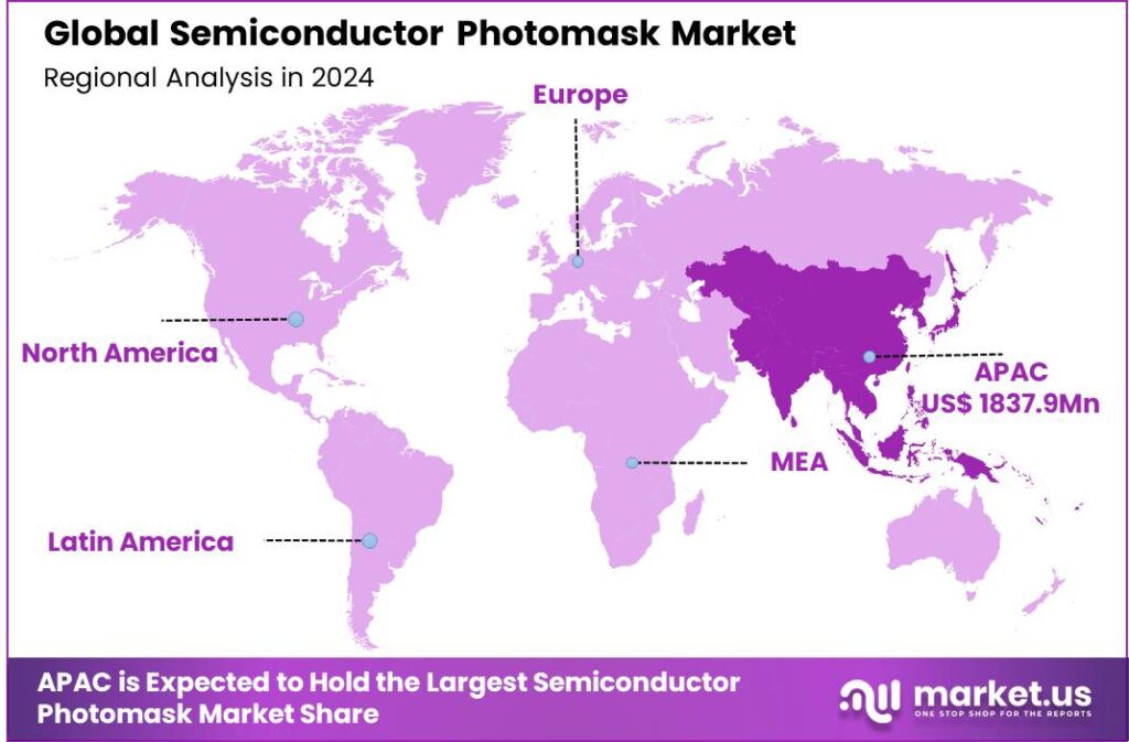
The Global Semiconductor Photomask Market is projected to grow from USD 4,927.5 million in 2024 to USD 8,659 million by 2034, at a CAGR of 5.80%. In 2024, the Asia-Pacific region led the market with over 37.3% share, generating approximately USD 1,837.9 million in revenue. China is expected to contribute USD 735.18 million, growing at a rate of 6.13% CAGR.
The growth of the semiconductor photomask market is driven by the rising demand for advanced electronics, fueled by advancements in consumer electronics, automotive tech, and IoT. Additionally, the shrinking of semiconductor technology to nanometer scales requires higher precision in photomasks, driving innovation in materials and production techniques.
Emerging trends in the semiconductor photomask market include the development of extreme ultraviolet (EUV) photomasks, which allow for smaller feature sizes and more densely packed circuits on a chip. This technology is becoming increasingly vital as the semiconductor industry pushes towards 5-nanometer and smaller nodes. Additionally, the shift towards multi-patterning techniques to achieve finer resolutions without transitioning to prohibitively expensive new equipment setups is another significant trend.
The market presents several key opportunities such as there is significant potential for growth in the adoption of EUV photomasks as the industry continues to innovate at the cutting edge of technology. Additionally, the market could see substantial expansions through investments in developing regions that are beginning to build their semiconductor manufacturing capabilities. Companies positioned to provide scalable solutions can leverage these opportunities for substantial growth.
Key challenges facing the semiconductor photomask industry include high production costs, especially concerning advanced masks like those used in EUV lithography. The complexity and precision required for these masks demand significant investments in technology and expertise. Another challenge is the rapid pace of technological change, which can render existing mask technologies obsolete, forcing continuous innovation and upgrades.
The market for semiconductor photomasks is poised for expansion across several regions. As countries and regions like China and Southeast Asia ramp up their semiconductor production capabilities, the demand for photomasks will likely increase. Furthermore, as technologies such as AI, 5G, and autonomous vehicles require more advanced semiconductor chips, the need for innovative photomask technologies will continue to grow, potentially leading to expanded market reach and the development of new production facilities.
Key Takeaways
- The global semiconductor photomask market is projected to grow from USD 4,927.5 million in 2024 to USD 8,659 million by 2034, at a CAGR of 5.80%.
- In 2024, the Reticle segment led the market, accounting for over 61.3% of the global share.
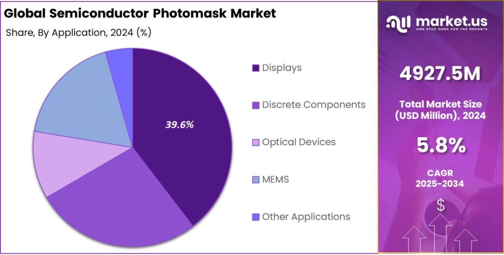
- The Displays segment held a significant position, representing more than 39.6% of the market in 2024.
- Asia-Pacific (APAC) held a key portion of the market, with 37.3% of the global share and contributing around USD 1.84 million in revenue in 2024.
- China’s semiconductor photomask market is expected to reach USD 735.18 million by 2024, growing at a CAGR of 6.13%.
Impact Of AI On The Market
- Enhancing Design and Manufacturing: AI technologies are increasingly being integrated into the design and manufacturing processes of photomasks. By analyzing large datasets, AI helps optimize semiconductor architectures, improve the performance of chip-enabled devices, and automate verification processes to ensure reliability in complex designs.
- Driving Demand for Advanced Photomasks: The rise of technologies such as extreme ultraviolet (EUV) lithography demands photomasks with extremely fine features. AI’s role in developing advanced semiconductors for applications like 5G, IoT, and AI itself fuels the need for more sophisticated photomasks that can support high-performance requirements.
- Reducing Manufacturing Time and Costs: AI is being used to streamline photomask production processes, reducing lead times and material wastage. This efficiency boost is crucial in an industry where precision and speed are paramount. Predictive maintenance powered by AI also helps minimize downtime and enhance productivity at manufacturing sites.
- Impact on Market Growth: The global photomask market is experiencing growth driven by the demand in consumer electronics and the automotive industry, where photomasks are essential for producing the semiconductor components used in complex systems like sensors and safety devices. North America and Asia-Pacific are notable regions leading this expansion due to their robust semiconductor manufacturing capabilities.
- Future Opportunities: As the semiconductor industry continues to innovate, AI will play a critical role in the development of next-generation photomasks. The integration of AI with other emerging technologies such as digital twins and IoT applications is likely to open up new avenues for the application of photomasks in various industries, further propelling market growth.
China Market Size and Growth
The market for semiconductor photomasks in China is anticipated to achieve a valuation of USD 735.18 million by 2024, exhibiting a compound annual growth rate (CAGR) of 6.13%. This growth trajectory underscores the robust expansion within the sector, driven by the escalating demand for more sophisticated semiconductor components across various industries.
Several factors are driving the surge in the semiconductor photomask market. Key among them are technological advancements and increased local manufacturing capabilities, allowing China to reduce its dependence on foreign imports and support domestic growth. The expanding electronics industry, particularly the rise in production of smartphones, tablets, and smart devices, further fuels the demand for high-precision photomasks. Additionally, government initiatives, including substantial investments and favorable policies, are boosting China’s semiconductor sector and enhancing its global competitiveness.
In 2024, the Asia-Pacific (APAC) region maintained a leading position in the global semiconductor photomask market, accounting for more than 37.3% of the worldwide market share. This dominance translated to a revenue contribution of around USD 1837 Million, highlighting APAC’s significant role in this sector.
The prominence of APAC in the semiconductor photomask market can be attributed to several key factors. Rapid industrialization across major APAC economies, coupled with substantial investments in the semiconductor industry, has propelled the region to the forefront. Moreover, the presence of leading semiconductor production hubs in countries such as South Korea, Taiwan, and China fuels the demand for photomasks, which are essential components in the fabrication of semiconductor devices.
Furthermore, the strategic initiatives by governments in the region to support the semiconductor industry through subsidies, tax incentives, and robust intellectual property protections have enhanced production capacities and technological advancements. These efforts solidify APAC’s role in the semiconductor photomask market, ensuring continued growth in the future.
You May Also Like To Read
- Semiconductor Wafer Inspection Equipment Market
- Semiconductor Lithography Equipment Market
- Semiconductor OHT (Overhead Hoist Transport) Market
- Outsourced Semiconductor Assembly and Test (OSAT) Market
- Semiconductor Recycling & Sustainability Market
Market Segmentation
Product Analysis
In 2024, the Reticle segment dominated the semiconductor photomask market, accounting for over 61.3% of the global market share. Reticles are essential for the photolithography process in semiconductor manufacturing, where they are used to project circuit patterns onto wafers. The dominance of this segment is driven by the increasing demand for smaller and more powerful semiconductor devices. With advancements in semiconductor technology and the shift toward smaller node processes (such as 5nm and below), the need for high-precision reticles has grown significantly.
Application Analysis
The Displays segment held a significant share of the semiconductor photomask market in 2024, capturing more than 39.6% of the market. This segment is primarily driven by the increasing demand for advanced display technologies, such as OLED, LCD, and micro-LED displays, which require photomasks for the precise patterning of pixels. The proliferation of large-screen televisions, smartphones, and wearable devices has led to an increased need for high-quality displays.
Key Market Segments
By Product
- Reticle
- Master
- Other Products
By Application
- Displays
- Discrete Components
- Optical Devices
- MEMS
- Other Applications
Emerging Trends
- Computational Lithography: Advanced computational methods, including optical proximity correction and source mask optimization, are being employed to enhance photomask performance and achieve finer feature resolutions.
- Resolution Enhancement Technologies (RET): Techniques like phase-shift masks and optical proximity correction are being utilized to improve the resolution of photomasks, allowing for the creation of smaller and more precise features on semiconductor wafers.
- Extreme Ultraviolet Lithography (EUVL): The adoption of EUV lithography is allowing for the patterning of extremely small features on photomasks, which is essential for producing advanced semiconductor devices with higher performance and lower power consumption.
- Advancements in Photomask Materials: Innovations in photomask materials, such as the use of more durable and precise substrates, are enhancing the durability and accuracy of photomasks, leading to improved yields in semiconductor manufacturing.
- Global Market Growth: The semiconductor photomask market is experiencing steady growth, driven by increasing demand for semiconductors in various industries, including consumer electronics, automotive, and telecommunications.
Top Use Cases
- Integrated Circuit Fabrication: Photomasks are fundamental in transferring circuit designs onto semiconductor wafers during lithography, enabling the creation of complex microchips used in various electronic devices.
- Micro-Electro-Mechanical Systems (MEMS) Production: In MEMS manufacturing, photomasks define micro-scale mechanical structures, such as sensors and actuators, facilitating their integration into electronic systems.
- Display Technology Manufacturing: Photomasks are utilized to pattern thin-film transistors and color filters in display panels, contributing to the production of high-resolution screens for televisions, smartphones, and monitors.
- Photonic Device Fabrication: In photonics, photomasks help create waveguides and optical components on semiconductor substrates, essential for fiber-optic communications and integrated photonic circuits.
- Advanced Packaging and IC Bumping: Photomasks are employed in defining patterns for solder bumps and redistribution layers in advanced semiconductor packaging, enhancing electrical connections and performance of integrated circuits.
Major Challenges
- Mask Defects: Tiny imperfections, even at the atomic scale, can lead to defects in the final semiconductor product. These defects may be buried within the multilayer structure of the mask, making them difficult to detect and correct.
- Multilayer Reflectivity Variations: Slight inconsistencies in the thickness of the molybdenum and silicon layers can cause significant local reflectivity variations. These variations are challenging to detect but can adversely affect the critical dimensions of semiconductor features.
- Pellicle Durability: Pellicles, which protect masks from contamination, must be extremely thin to avoid excessive EUV light absorption. However, they can deform or fail under high-power EUV exposure, leading to particle contamination and reduced yield.
- Hydrogen-Induced Blistering: Exposure to hydrogen, used in cleaning processes, can penetrate mask layers and cause blistering or peeling. This degradation affects the mask’s integrity and can lead to defects in the semiconductor devices.
- Shadowing Effects: The off-axis illumination in EUV lithography causes shadowing, leading to asymmetry in the diffraction pattern. This asymmetry can degrade pattern fidelity, making it challenging to accurately reproduce the intended semiconductor features.
Market Opportunities for Key Players
- Advancements in Semiconductor Technology: As the industry moves towards smaller nodes and more sophisticated chip designs, such as 3D stacking and FinFET, the demand for high-precision photomasks is increasing. These masks are critical for producing intricate chip features essential in modern electronics.
- Emerging Technologies: The surge in demand for semiconductor chips in AI, machine learning, and quantum computing offers substantial opportunities. These fields require advanced chips with complex architectures that necessitate precision photomasks.
- Next-Generation Lithography Techniques: Techniques like Extreme Ultraviolet (EUV) lithography and multi-patterning are advancing, which requires photomasks that can support smaller and more complex patterns. This trend is pushing the demand for innovative photomask technologies.
- Regional Expansion in Semiconductor Production: With increasing investments in semiconductor fabrication facilities across the U.S., Europe, and Southeast Asia, there is a growing need for advanced photomasks to support localized manufacturing efforts.
- Custom Photomask Solutions: There is a growing trend towards custom photomasks tailored to specific customer needs. This customization allows photomask companies to provide solutions that fit unique requirements, offering a competitive edge in the market.
Report Scope
| Report Features | Description |
| Market Value (2024) | USD 4,927.5 Mn |
| Forecast Revenue (2034) | USD 8,659 Mn |
| CAGR (2025-2034) | 5.80% |
| Base Year for Estimation | 2024 |
| Historic Period | 2020-2023 |
| Forecast Period | 2025-2034 |
Conclusion
In conclusion, the semiconductor photomask market is poised for substantial growth, driven by the increasing demand for advanced semiconductor devices in various industries such as electronics, automotive, and telecommunications. The market is driven by the growing adoption of technologies like 5G, AI, and IoT, which demand smaller, more complex semiconductors. The expansion of manufacturing capabilities and miniaturization further boosts the demand for photomasks, crucial for precise pattern transfer in lithography.
Furthermore, innovations in photomask technology, including the development of extreme ultraviolet (EUV) lithography masks, are expected to further propel market expansion. As manufacturers aim to boost production efficiency and performance, the photomask production market will evolve, with a growing emphasis on accuracy and cost-effectiveness. This creates significant growth opportunities, particularly in Asia-Pacific, a key hub for semiconductor manufacturing.
Discuss your needs with our analyst
Please share your requirements with more details so our analyst can check if they can solve your problem(s)